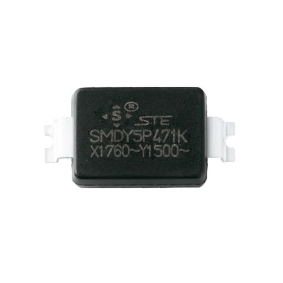
SMD-X1Y1SMD

SMD-X1Y1 Series Safety Certified SMD Ceramic Capacitors (Class X1/Y1)

Safety classX1 / Y1 (IEC 60384-14)
Rated voltageX1 760 VAC · Y1 500 VAC
Capacitance10–4,700 pF
Package format3022 / 3222 / 3225 / 4522
ApprovalsCQC · VDE/ENEC · UL/cUL · IEC CB · KTL
VDE certification markENEC certification mark

Resin-molded SMD ceramic safety capacitors, Class X1/Y1, for EMI suppression. X1 760 VAC, Y1 500 VAC, 10–4,700 pF.

SMD-X1Y1 safety ceramic product photograph

Part numbers and datasheets

Part numbers and datasheets on request. Tell us the application, your specifications and the expected volume, and an STE engineer will reply by email.

Already have an STE part number? Search STE part numbers

Engineering details

Overview

Resin-molded SMD ceramic safety capacitors, Class X1/Y1 to IEC 60384-14, for AC-line EMI suppression and primary-to-secondary coupling in low-profile power supplies. Rated X1 760 VAC / Y1 500 VAC, 10–4,700 pF, in four SMD package formats, 2.4–2.5 mm high. Operating temperature −40 °C to +125 °C.

Series features

  • Class X1/Y1 to IEC 60384-14, for circuit positions that require reinforced insulation
  • Body height 2.4–2.5 mm; flat terminals, no leads through the board
  • Dielectric withstand 4 kVAC r.m.s. between terminals, 60 s
  • Tape and reel, MSL 3, reflow solderable, for automated SMT assembly
  • Flame-retardant epoxy molding to UL 94 V-0
Specifications
Safety classX1 / Y1 (IEC 60384-14)
Rated voltageX1 760 VAC · Y1 500 VAC
Capacitance range10–4,700 pF
Package formats3022 · 3222 · 3225 · 4522 (STE format codes, not EIA chip sizes)
Operating temperature−40 °C to +125 °C
Climatic category40/125/21 · flammability class B
DielectricsSL · Y5P · Y5U · Y5V
Capacitance toleranceK ±10% · M ±20%
Dielectric withstand4 kVAC r.m.s. · 60 s
Insulation resistance>10,000 MΩ at 500 VDC, 60 ±5 s
Moisture sensitivityMSL 3
FlammabilityEpoxy molding to UL 94 V-0
Variants

Ranges by dielectric, package and lead style within this series.

VariantBody dimensionsCapacitanceDielectricLead / land patternNotes
3022L 7.8 ±0.3 · W 5.4 ±0.2 · H 2.4 ±0.2 mm10–2,200 pFSL · Y5P · Y5U · Y5Va ≥8.0 · b 2.2 ±0.1 · c 3.6 ±0.1 mmShortest body, for low-profile, space-constrained layouts.
3222L 8.1 ±0.3 · W 5.5 ±0.3 · H 2.5 ±0.3 mm10–2,200 pFSL · Y5P · Y5U · Y5Va 10.0 ±0.2 · b 2.2 ±0.2 · c 3.6 ±0.2 mmGeneral low-profile format with 10 mm land span.
3225L 8.1 ±0.3 · W 6.0 ±0.3 · H 2.5 ±0.3 mm10–2,200 pFSL · Y5P · Y5U · Y5Va 10.0 ±0.2 · b 2.2 ±0.2 · c 3.6 ±0.2 mmWider body; covers the main 10–2,200 pF range.
4522L 11.5 ±0.3 · W 6.1 max. · T 2.5 ±0.3 mm3,300–4,700 pFY5Va 9.0 ±0.2 · b 1.7 ±0.2 · c 3.6 ±0.2 mmHigher-capacitance format for 3.3 nF and 4.7 nF.
Selection guide

Choose the safety position first, then capacitance and dielectric, then the package format. Package codes are STE format names, not EIA chip sizes. Land pattern and approval scope: see the datasheet.

  1. Confirm the X1 or Y1 position

    Define whether the capacitor sits line-to-line, line-to-earth or across an isolation barrier. A Y1 position requires the matching safety approval and insulation coordination in the end equipment.

  2. Define the voltage envelope

    Include nominal AC voltage, switching overshoot, surges and abnormal conditions. The 4 kVAC withstand is a test condition, not a continuous working-voltage rating.

  3. Choose capacitance and dielectric

    SL covers the lowest values with the highest stability; Y5P, Y5U and Y5V extend capacitance in that order. Capacitance change over temperature and tolerance: see the datasheet.

  4. Verify footprint and creepage

    Use the body and land dimensions of the selected package. Recheck creepage and clearance on the assembled PCB, including pollution degree, coating and spacing to the chassis.

  5. Validate the assembly process

    Handle the series as MSL 3, validate the reflow profile and observe the floor life after opening the bag. Confirm cleaning agents, coatings and potting compounds on the production assembly.


Approvals & reliability

Approvals & qualifications

Approved ratings differ by agency.

AgencyStandardCertificateScope
CQC certification markCQCIEC 60384-14:2013 + AMD1:2016CQC24001446247SMD X1/Y1, 10–4,700 pF. Issued 2 Feb 2026, valid to 1 Feb 2031 subject to surveillance.
VDE certification markENEC certification markVDE / ENECIEC / EN IEC 60384-14:202340058861Rated voltage: X1 760 / 500 / 400 VAC; Y1 500 / 400 / 250 VAC
UL certification markUL / cULUL / CSA 60384-14E530201Recognized component, USA and Canada.
IECEE CB scheme markIEC CBIEC 60384-14:2023DE1-68874/B1CB Scheme test certificate
KTL organization logoKTLKC 60384-1 / KC 60384-14SU03031-24001BRated voltage: Y1 250 VAC

Each certificate covers the types and ratings listed on it.

Reliability tests

Test conditions and acceptance limits. Limits can vary by package and dielectric; see the datasheet.

TestConditionAcceptance
Damp heat, steady state40 ±2 °C · 90–95% RH · 500 ±12 hNo visible damage · ΔC within the specified limit · IR >5,000 MΩ · withstands 4 kVAC, 60 s
Damp heat with load40 ±2 °C · 90–95% RH · rated voltage · 500 ±12 hNo visible damage · electrical limits met after the test
Endurance125 °C · 1,000 h · test voltage with hourly impulse per datasheetNo visible damage · ΔC within ±20% · IR >5,000 MΩ · withstands 4 kVAC, 60 s
Rapid change of temperature−40 °C ↔ +125 °C · five cyclesNo visible damage · capacitance and dissipation factor within the limits of the dielectric
Resistance to soldering heatSolder 260 +5/−0 °C · 10 ±1 s · after preconditioningNo visible damage · ΔC within ±10% · withstands 4 kVAC, 60 s
Vibration, board bending and shear10–55–10 Hz · 1.5 mm · 6 h; bend and 5 N shear test per packageNo significant abnormality or terminal displacement; electrical drift within the specified limits
Design notes

Reflow and moisture handling

MSL 3. Store at ≤30 °C / 60% RH and use within six months of delivery. Complete soldering within 168 h after opening the moisture barrier bag. If floor life or storage time is exceeded, bake at 60 °C for 168 h. Reference reflow window: 230–260 °C for 10–30 s, preheat 170 °C max. Validate the production profile.

Working voltage and self-heating

Keep all steady-state and transient voltage components within the rated voltage. Keep the capacitor surface below the +125 °C operating limit, including self-heating from dielectric loss. For the applicable high-permittivity dielectrics, limit temperature rise to 20 °C at 25 °C ambient.

PCB land, flex and handling

Match the land pattern to the selected package. Do not move, tilt or load the body after soldering. Board flex, terminal misalignment and mechanical shock can damage the ceramic element or the termination.

Cleaning, coating and potting

Validate cleaning agents, adhesives, conformal coatings and potting resins on the actual assembly. Organic solvents and mismatched curing or thermal expansion can attack the epoxy or cause cracks during temperature cycling.

Dielectric-withstand testing

Use a 50/60 Hz sinusoidal source, secure the terminals and ramp up from near zero. Repeated hipot testing can damage the component. Do not return parts used for hipot verification to production stock.

Fail-safe design

A damaged safety capacitor can fail short. Provide fusing or another automatic protective function. Contact STE before use in life-support, transportation, power-plant control or other applications where failure has severe consequences.