SMD-DCSMD

SMD-DC Series Medium & High Voltage SMD Ceramic Capacitors

Rated voltage1 / 2 / 3 kVDC
Capacitance10–4,700 pF
Package format1815 / 2522
DielectricsSL · Y5P · Y5U · Y5V

Resin-molded SMD ceramic capacitors for high-voltage DC circuits. Rated 1,000, 2,000 and 3,000 VDC, 10–4,700 pF, in 1815 and 2522 formats.

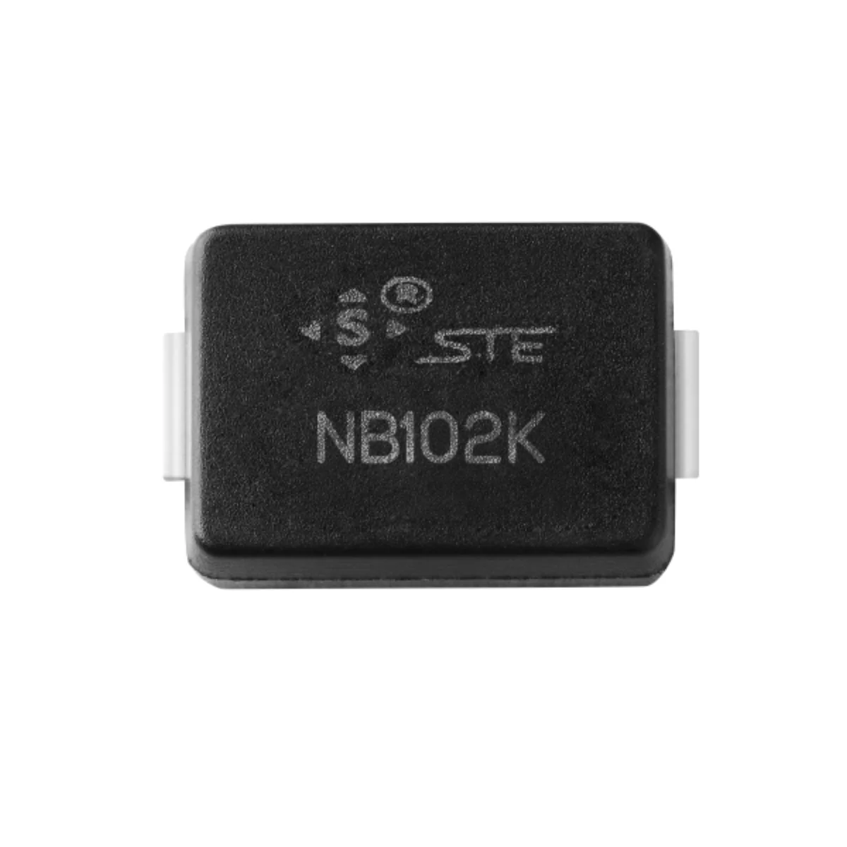
SMD high-voltage ceramic product photograph

Part numbers and datasheets

Part numbers and datasheets on request. Tell us the application, your specifications and the expected volume, and an STE engineer will reply by email.

Engineering details

Overview

Resin-molded SMD ceramic capacitors for 1–3 kVDC circuits. Rated 1,000, 2,000 or 3,000 VDC, 10–4,700 pF, in 1815 and 2522 formats with 2.2–2.38 mm nominal body height. Dielectrics SL, Y5P, Y5U and Y5V; MSL 3, tape and reel. DC components, not X/Y safety capacitors.

Series features

  • Rated voltage 1,000, 2,000 or 3,000 VDC
  • Nominal body height 2.2–2.38 mm; flat terminals, no leads through the board
  • Withstand voltage and insulation resistance specified per dielectric
  • 3,000 pcs per reel, MSL 3, reflow solderable
  • Flame-retardant epoxy molding to UL 94 V-0
Specifications
Rated voltage1,000 · 2,000 · 3,000 VDC
Capacitance range10–4,700 pF, depending on package
Package formats1815 · 2522 (STE format codes, not EIA chip sizes)
DielectricsSL · Y5P · Y5U · Y5V, depending on package
Capacitance toleranceK ±10% · M ±20%
Dissipation factorSL ≤0.1% · Y5P/Y5U/Y5V ≤2.5%
Withstand voltage, 1 kV, SL1.5 × UR · 1–5 s
Withstand voltage, 1 kV, Class 22 × UR · 1–5 s
Withstand voltage, 2 kV and 3 kV1.5 × UR + 500 V · 1–5 s
Insulation resistanceSL >10,000 MΩ · Class 2 >4,000 MΩ
IR test condition500 VDC · 60 ±5 s · charge/discharge current ≤50 mA
Moisture sensitivityMSL 3
Reel quantity3,000 pcs
Endurance test1.5 × UR · 105 ±2 °C · 1,000 h
FlammabilityEpoxy molding to UL 94 V-0
Variants

Ranges by dielectric, package and lead style within this series.

VariantBody dimensionsCapacitanceDielectricLead / land patternNotes
1815L 4.5 ±0.3 · W 3.9 ±0.3 · H 2.2 ±0.3 mm10–2,200 pFSL · Y5P · Y5U · Y5Va ≥4.0 · b 2.2 ±0.1 · c 3.2 ±0.2 mmSmallest format; the only format with SL values of 10–68 pF.
2522L 6.0 ±0.1 · W 5.55 ±0.1 · H 2.38 ±0.1 mm390–4,700 pFY5P · Y5U · Y5Va ≥5.5 · b 2.2 ±0.1 · c 3.6 ±0.2 mmHigher-capacitance format up to 4.7 nF.
Selection guide

Choose the voltage code and dielectric before optimizing capacitance. The series is a high-voltage DC component, not an IEC 60384-14 safety capacitor. Package codes are STE format names, not EIA chip sizes.

  1. Define the actual DC stress

    Add DC bias, ripple peak, switching overshoot, start-up and fault transients. Keep the complete waveform within the rated voltage. The withstand-test voltage is not a continuous working rating.

  2. Choose voltage code N, R or S

    N = 1 kVDC, R = 2 kVDC, S = 3 kVDC. Not all capacitance, dielectric and voltage combinations are available.

  3. Choose the dielectric for the required stability

    SL gives the lowest dissipation factor and the highest insulation resistance at low capacitance. Y5P, Y5U and Y5V extend capacitance, with increasingly wide capacitance change over temperature.

  4. Choose the package

    1815 covers 10–2,200 pF and includes SL; 2522 covers 390–4,700 pF. Verify body, land span, PCB creepage and clearance for the applied voltage and environment.

  5. Validate circuit and assembly stresses

    Check ripple and self-heating, pulse energy, board flex, contamination and coating. Apply MSL 3, reflow and post-solder handling controls on the production assembly.

Approvals & reliability

Reliability tests

Test conditions and limits by dielectric. Test voltages and temperatures are test conditions, not continuous operating ratings.

TestConditionAcceptance
Damp heat, steady state40 ±2 °C · 90–95% RH · 500 +24/−0 hNo visible damage · capacitance and DF within dielectric limits · IR: SL >5,000 MΩ, Class 2 >2,000 MΩ
Damp heat with load40 ±2 °C · 90–95% RH · rated voltage · 500 +24/−0 hNo visible damage · capacitance, DF and IR within dielectric limits
Endurance105 ±2 °C · 1.5 × rated voltage · 1,000 +48/−0 hNo visible damage · ΔC: SL ≤±5%, Y5P/Y5U ≤±20%, Y5V ≤±30% · DF and IR within limits after test
Temperature cycling−25 °C ↔ +105 °C · five cycles, after preconditioning at 85 °CNo visible damage; marking legible after recovery
Resistance to soldering heatPreheat 150–180 °C, 90 ±30 s · reflow 230–260 °C, 60 ±15 s · four cyclesNo visible damage · capacitance and IR within dielectric limits · no breakdown or flashover
Mechanical robustnessVibration 10–55 Hz, 1.5 mm · shock 490 m/s², 11 ms · terminal shear 10 NNo visible damage or terminal displacement; capacitance change within the specified limit
Design notes

Not a safety capacitor

This DC-rated series is not an X/Y safety capacitor. Its rated or withstand voltage does not imply line-to-earth, line-to-line or reinforced-insulation approval. Where the equipment standard requires a safety capacitor, select a certified X/Y series.

Voltage waveform and derating

Keep DC bias plus ripple and all repetitive or abnormal peaks within the rated voltage. Set derating from the equipment environment, expected lifetime, contamination and transient spectrum. A 1–5 s withstand test is not a design margin.

Reflow and moisture handling

MSL 3. Store at ≤30 °C / 60% RH, use within six months and solder within 168 h after opening. If storage time or floor life is exceeded, bake at 60 °C for 168 h. Reference reflow window: 230–260 °C for 10–30 s, preheat 170 °C max.

Self-heating and pulse use

Measure the surface temperature under the real voltage waveform, with nearby heat-generating parts in place. For the applicable Class 2 dielectrics, limit temperature rise from dielectric loss to 20 °C at 25 °C ambient. Pulse-current and energy ratings are not specified for the series; validate snubber or resonant use in the application.

PCB layout and mechanical stress

Use the land dimensions of the selected package and verify creepage and clearance for the applied voltage. Avoid board flex, terminal misalignment, body movement after soldering and impact; they can crack the ceramic or the termination.

Cleaning, coating and fail-safe design

Validate cleaning agents, adhesives, coatings and potting resins on the actual assembly; solvents or thermal-expansion mismatch can damage the epoxy or the ceramic. Provide fusing or another protective function where a shorted capacitor could cause electric shock, fire or smoke.