
STE Introduces 3225 and 4032 SMD Varistors for Compact Protection Circuits
Original report
STE edition
Chongdiantou’s introduction covers two STE SMD varistor packages, their reported electrical ranges and packaging for automated assembly.
Chongdiantou reported on April 29, 2025 that STE had introduced surface mount varistors in 3225 and 4032 packages. The announcement addressed demand for compact protection components in LED products, industrial equipment, communications devices, household appliances and power adapters.
The report presented the range as an extension of STE's capacitor, varistor and thermistor portfolio. Its main product themes were a smaller mounting outline, compatibility with automated assembly and transient-overvoltage protection. This English adaptation preserves the reported product information while separating announcement values from the conditions required for component selection.
Two packages in the reported range
A varistor has a nonlinear voltage-current characteristic. It carries relatively little current within its intended normal operating conditions and conducts more strongly during an overvoltage event. The voltage remaining across it depends on the current and waveform, so its nominal varistor voltage must not be treated as a fixed clamping voltage.
Chongdiantou gave the following comparison for the two STE packages:
| Parameter reported in April 2025 | 3225 | 4032 |
|---|---|---|
| Body length × width | 8.0 × 6.3 mm | 10.75 × 8.2 mm |
| Nominal varistor-voltage range | 200–820 V | 200–820 V |
| Varistor-voltage tolerance | ±10% | ±10% |
| Operating temperature range | −40 to +125°C | −40 to +125°C |
| Reported maximum peak current | 1750 A | 3500 A |
| Reported energy range | 17–73 J | 35–110 J |
| Reported rated power | 0.25 W | 0.4 W |
These are historical values from the linked report. Use the part-specific STE SMD-MOV specification for design selection. The accompanying product tables specify an 8/20 µs waveform for peak current and a 10/1000 µs waveform for energy. Pulse-count conditions are part-specific and must be read with each table entry. These figures are not continuous current limits.
Likewise, the 200–820 V range describes nominal varistor voltage, not the allowable continuous AC supply range. A design decision needs the selected device's maximum continuous voltage, clamping data and temperature limits together. The reported package dimensions also do not replace a toleranced terminal and land-pattern drawing.
Assembly and packaging details
The announcement described molding material meeting UL94 V-0 and suitability for the specified lead-free reflow or wave-soldering processes. A material flammability classification is distinct from certification of the complete component or the equipment containing it.
The packaging figures were specific: 3225 devices used 16 mm carrier tape, while 4032 devices used 24 mm tape. Both were supplied in reels of 1500 pieces. The reported carton configurations were 11 reels, or 16,500 pieces, for 3225 and six reels, or 9000 pieces, for 4032.
Those formats support automated feeding and placement. Production benefits depend on the actual footprint, soldering profile and assembly controls; the report does not provide a measured comparison of manufacturing yield or cost.
Applications depend on the protection circuit
Chongdiantou highlighted power adapters, lighting and industrial or communications electronics as potential uses. It also referred to temperature and humidity performance and reliability testing. The linked report can be consulted for its original illustrations, but the available text does not establish a complete qualification record or automotive approval for the range.
For an intended application, the next step is to obtain the current specification for the exact SMD variant and review it alongside the required equipment surge test, downstream voltage tolerance and fault protection. A successful component test under defined conditions is useful evidence; it does not, by itself, establish the surge performance of the complete product.
Figures and tables from the original report
The following figures retain their original captions, markings and historical context. Transcribed tables present the values shown in the published images; product selection should use the specifications for the selected part.
| Field | Source description |
|---|---|
| Mounting type | SMD |
| Component type | MOV: metal-oxide varistor |
| Approximate body dimensions | 3225≈8.0×6.3 mm; 4032≈10.75×8.2 mm |
| Varistor-voltage tolerance | K: ±10% |
| Varistor-voltage codes | 201: 200 V; 821: 820 V |
| Item | Source statement |
|---|---|
| Source feature 1 | Molded package; the source states that the encapsulation material meets UL94-V0. |
| Source feature 2 | Compact package intended to save board space. |
| Source feature 3 | The source describes resistance to high temperature and humidity. |
| Source feature 4 | The source describes high surge-current suppression capability. |
| Source feature 5 | Reel packaging for automated assembly using lead-free reflow or wave soldering. |
| Applications listed by the source | LED circuit protection, industrial equipment, communications equipment, household appliances and power supplies. |
These are statements in the historical source image, not independent verification of certification, environmental testing or automotive qualification. Check the specific device soldering profile before assembly.
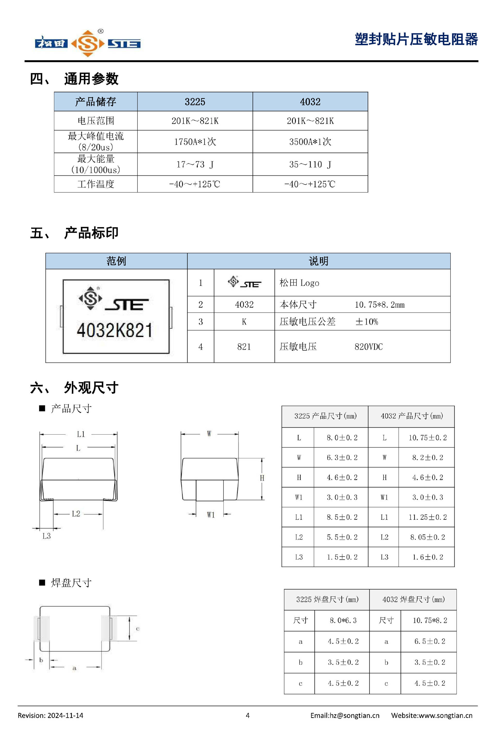
| Parameter | 3225 | 4032 |
|---|---|---|
| Voltage range (source codes) | 201K–821K | 201K–821K |
| Maximum peak current (8/20 μs) | 1750 A, 1 pulse | 3500 A, 1 pulse |
| Maximum energy (10/1000 μs) | 17–73 J | 35–110 J |
| Operating temperature | -40 to +125°C | -40 to +125°C |
The source first-column heading reads “product storage”; the English heading is normalized to Parameter. Historical image: revision 2024-11-14, page 4.
| No. | Marking | Meaning |
|---|---|---|
| 1 | STE logo | STE logo |
| 2 | 4032 | Body size: 10.75×8.2 mm |
| 3 | K | Varistor-voltage tolerance: ±10% |
| 4 | 821 | Varistor voltage: 820 VDC |
| Symbol | 3225 | 4032 |
|---|---|---|
| L | 8.0±0.2 | 10.75±0.2 |
| W | 6.3±0.2 | 8.2±0.2 |
| H | 4.6±0.2 | 4.6±0.2 |
| W1 | 3.0±0.3 | 3.0±0.3 |
| L1 | 8.5±0.2 | 11.25±0.2 |
| L2 | 5.5±0.2 | 8.05±0.2 |
| L3 | 1.5±0.2 | 1.6±0.2 |
| Symbol | 3225 | 4032 |
|---|---|---|
| Size | 8.0×6.3 | 10.75×8.2 |
| a | 4.5±0.2 | 6.5±0.2 |
| b | 3.5±0.2 | 3.5±0.2 |
| c | 4.5±0.2 | 4.5±0.2 |
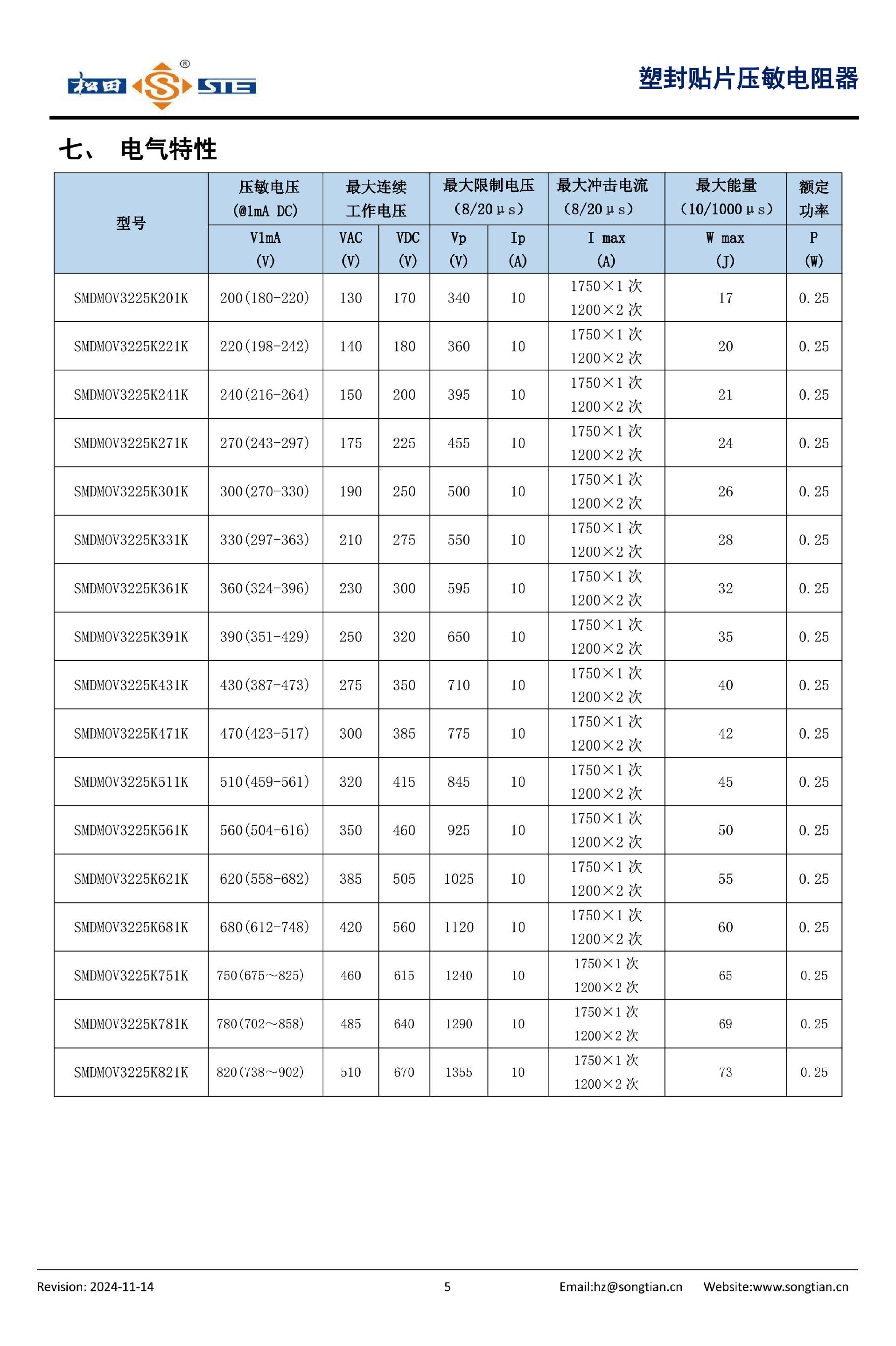
| Model | Varistor voltage V1mA at 1 mA DC (V) | Maximum continuous AC voltage (V) | Maximum continuous DC voltage (V) | Maximum clamping voltage Vp, 8/20 μs (V) | Clamping test current Ip, 8/20 μs (A) | Maximum surge current Imax, 8/20 μs (A) | Maximum energy Wmax, 10/1000 μs (J) | Rated power P (W) |
|---|---|---|---|---|---|---|---|---|
| SMDMOV3225K201K | 200 (180–220) | 130 | 170 | 340 | 10 | 1750 × 1 pulse; 1200 × 2 pulses | 17 | 0.25 |
| SMDMOV3225K221K | 220 (198–242) | 140 | 180 | 360 | 10 | 1750 × 1 pulse; 1200 × 2 pulses | 20 | 0.25 |
| SMDMOV3225K241K | 240 (216–264) | 150 | 200 | 395 | 10 | 1750 × 1 pulse; 1200 × 2 pulses | 21 | 0.25 |
| SMDMOV3225K271K | 270 (243–297) | 175 | 225 | 455 | 10 | 1750 × 1 pulse; 1200 × 2 pulses | 24 | 0.25 |
| SMDMOV3225K301K | 300 (270–330) | 190 | 250 | 500 | 10 | 1750 × 1 pulse; 1200 × 2 pulses | 26 | 0.25 |
| SMDMOV3225K331K | 330 (297–363) | 210 | 275 | 550 | 10 | 1750 × 1 pulse; 1200 × 2 pulses | 28 | 0.25 |
| SMDMOV3225K361K | 360 (324–396) | 230 | 300 | 595 | 10 | 1750 × 1 pulse; 1200 × 2 pulses | 32 | 0.25 |
| SMDMOV3225K391K | 390 (351–429) | 250 | 320 | 650 | 10 | 1750 × 1 pulse; 1200 × 2 pulses | 35 | 0.25 |
| SMDMOV3225K431K | 430 (387–473) | 275 | 350 | 710 | 10 | 1750 × 1 pulse; 1200 × 2 pulses | 40 | 0.25 |
| SMDMOV3225K471K | 470 (423–517) | 300 | 385 | 775 | 10 | 1750 × 1 pulse; 1200 × 2 pulses | 42 | 0.25 |
| SMDMOV3225K511K | 510 (459–561) | 320 | 415 | 845 | 10 | 1750 × 1 pulse; 1200 × 2 pulses | 45 | 0.25 |
| SMDMOV3225K561K | 560 (504–616) | 350 | 460 | 925 | 10 | 1750 × 1 pulse; 1200 × 2 pulses | 50 | 0.25 |
| SMDMOV3225K621K | 620 (558–682) | 385 | 505 | 1025 | 10 | 1750 × 1 pulse; 1200 × 2 pulses | 55 | 0.25 |
| SMDMOV3225K681K | 680 (612–748) | 420 | 560 | 1120 | 10 | 1750 × 1 pulse; 1200 × 2 pulses | 60 | 0.25 |
| SMDMOV3225K751K | 750 (675~825) | 460 | 615 | 1240 | 10 | 1750 × 1 pulse; 1200 × 2 pulses | 65 | 0.25 |
| SMDMOV3225K781K | 780 (702~858) | 485 | 640 | 1290 | 10 | 1750 × 1 pulse; 1200 × 2 pulses | 69 | 0.25 |
| SMDMOV3225K821K | 820 (738~902) | 510 | 670 | 1355 | 10 | 1750 × 1 pulse; 1200 × 2 pulses | 73 | 0.25 |
Historical revision 2024-11-14. The source gives 190 V AC for 3225K301K and 195 V AC for 4032K301K; the 621 models have clamping values of 1025 V and 1020 V respectively. These differences are retained.
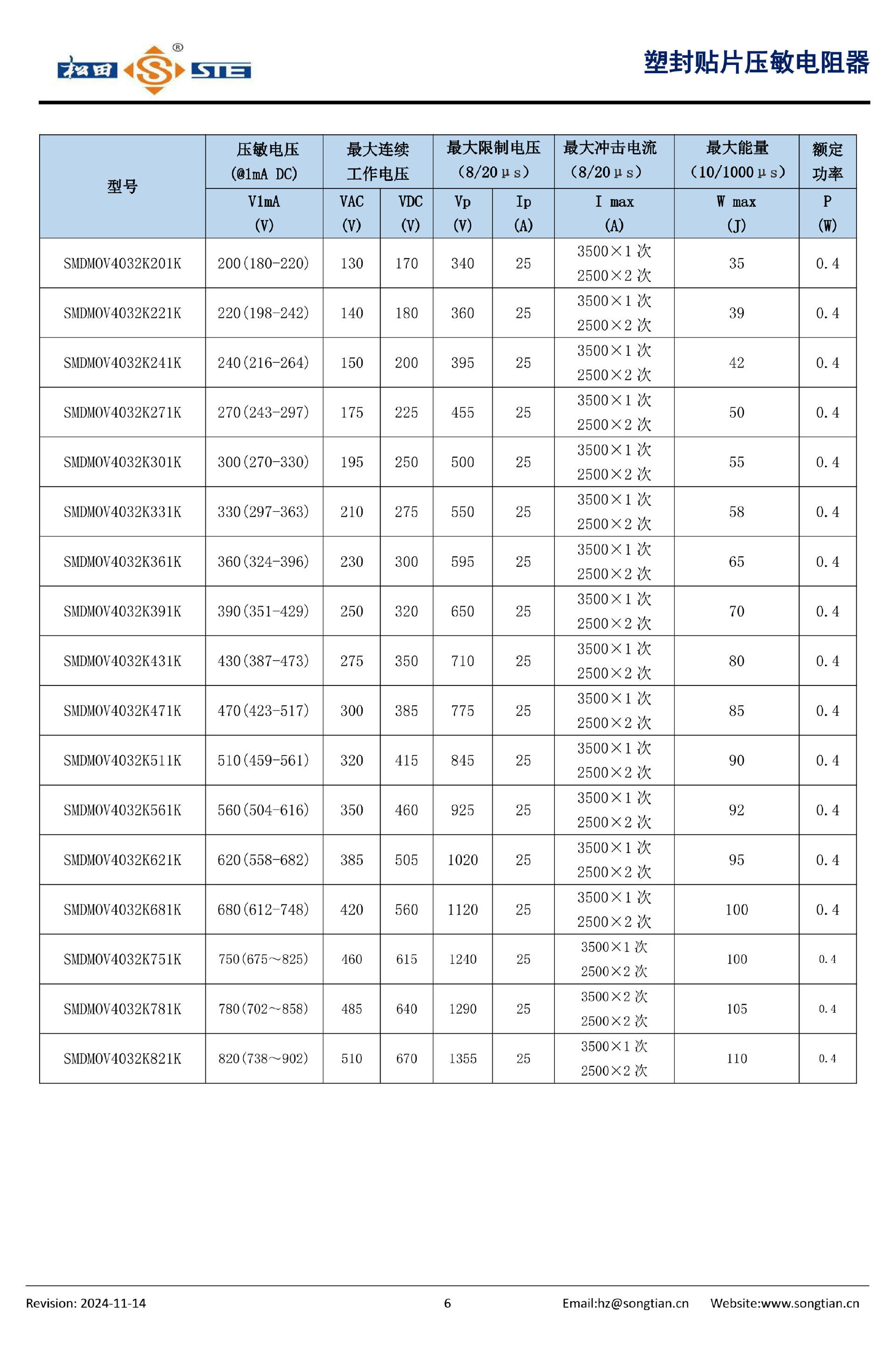
| Model | Varistor voltage V1mA at 1 mA DC (V) | Maximum continuous AC voltage (V) | Maximum continuous DC voltage (V) | Maximum clamping voltage Vp, 8/20 μs (V) | Clamping test current Ip, 8/20 μs (A) | Maximum surge current Imax, 8/20 μs (A) | Maximum energy Wmax, 10/1000 μs (J) | Rated power P (W) |
|---|---|---|---|---|---|---|---|---|
| SMDMOV4032K201K | 200 (180–220) | 130 | 170 | 340 | 25 | 3500 × 1 pulse; 2500 × 2 pulses | 35 | 0.4 |
| SMDMOV4032K221K | 220 (198–242) | 140 | 180 | 360 | 25 | 3500 × 1 pulse; 2500 × 2 pulses | 39 | 0.4 |
| SMDMOV4032K241K | 240 (216–264) | 150 | 200 | 395 | 25 | 3500 × 1 pulse; 2500 × 2 pulses | 42 | 0.4 |
| SMDMOV4032K271K | 270 (243–297) | 175 | 225 | 455 | 25 | 3500 × 1 pulse; 2500 × 2 pulses | 50 | 0.4 |
| SMDMOV4032K301K | 300 (270–330) | 195 | 250 | 500 | 25 | 3500 × 1 pulse; 2500 × 2 pulses | 55 | 0.4 |
| SMDMOV4032K331K | 330 (297–363) | 210 | 275 | 550 | 25 | 3500 × 1 pulse; 2500 × 2 pulses | 58 | 0.4 |
| SMDMOV4032K361K | 360 (324–396) | 230 | 300 | 595 | 25 | 3500 × 1 pulse; 2500 × 2 pulses | 65 | 0.4 |
| SMDMOV4032K391K | 390 (351–429) | 250 | 320 | 650 | 25 | 3500 × 1 pulse; 2500 × 2 pulses | 70 | 0.4 |
| SMDMOV4032K431K | 430 (387–473) | 275 | 350 | 710 | 25 | 3500 × 1 pulse; 2500 × 2 pulses | 80 | 0.4 |
| SMDMOV4032K471K | 470 (423–517) | 300 | 385 | 775 | 25 | 3500 × 1 pulse; 2500 × 2 pulses | 85 | 0.4 |
| SMDMOV4032K511K | 510 (459–561) | 320 | 415 | 845 | 25 | 3500 × 1 pulse; 2500 × 2 pulses | 90 | 0.4 |
| SMDMOV4032K561K | 560 (504–616) | 350 | 460 | 925 | 25 | 3500 × 1 pulse; 2500 × 2 pulses | 92 | 0.4 |
| SMDMOV4032K621K | 620 (558–682) | 385 | 505 | 1020 | 25 | 3500 × 1 pulse; 2500 × 2 pulses | 95 | 0.4 |
| SMDMOV4032K681K | 680 (612–748) | 420 | 560 | 1120 | 25 | 3500 × 1 pulse; 2500 × 2 pulses | 100 | 0.4 |
| SMDMOV4032K751K | 750 (675~825) | 460 | 615 | 1240 | 25 | 3500 × 1 pulse; 2500 × 2 pulses | 100 | 0.4 |
| SMDMOV4032K781K | 780 (702~858) | 485 | 640 | 1290 | 25 | 3500 × 2 pulses; 2500 × 2 pulses | 105 | 0.4 |
| SMDMOV4032K821K | 820 (738~902) | 510 | 670 | 1355 | 25 | 3500 × 1 pulse; 2500 × 2 pulses | 110 | 0.4 |
Historical revision 2024-11-14. The source gives 190 V AC for 3225K301K and 195 V AC for 4032K301K; the 621 models have clamping values of 1025 V and 1020 V respectively. These differences are retained. The 781K row prints 3500 × 2 pulses, unlike 3500 × 1 pulse in the other rows. This source anomaly is retained and does not establish a verified two-pulse rating.
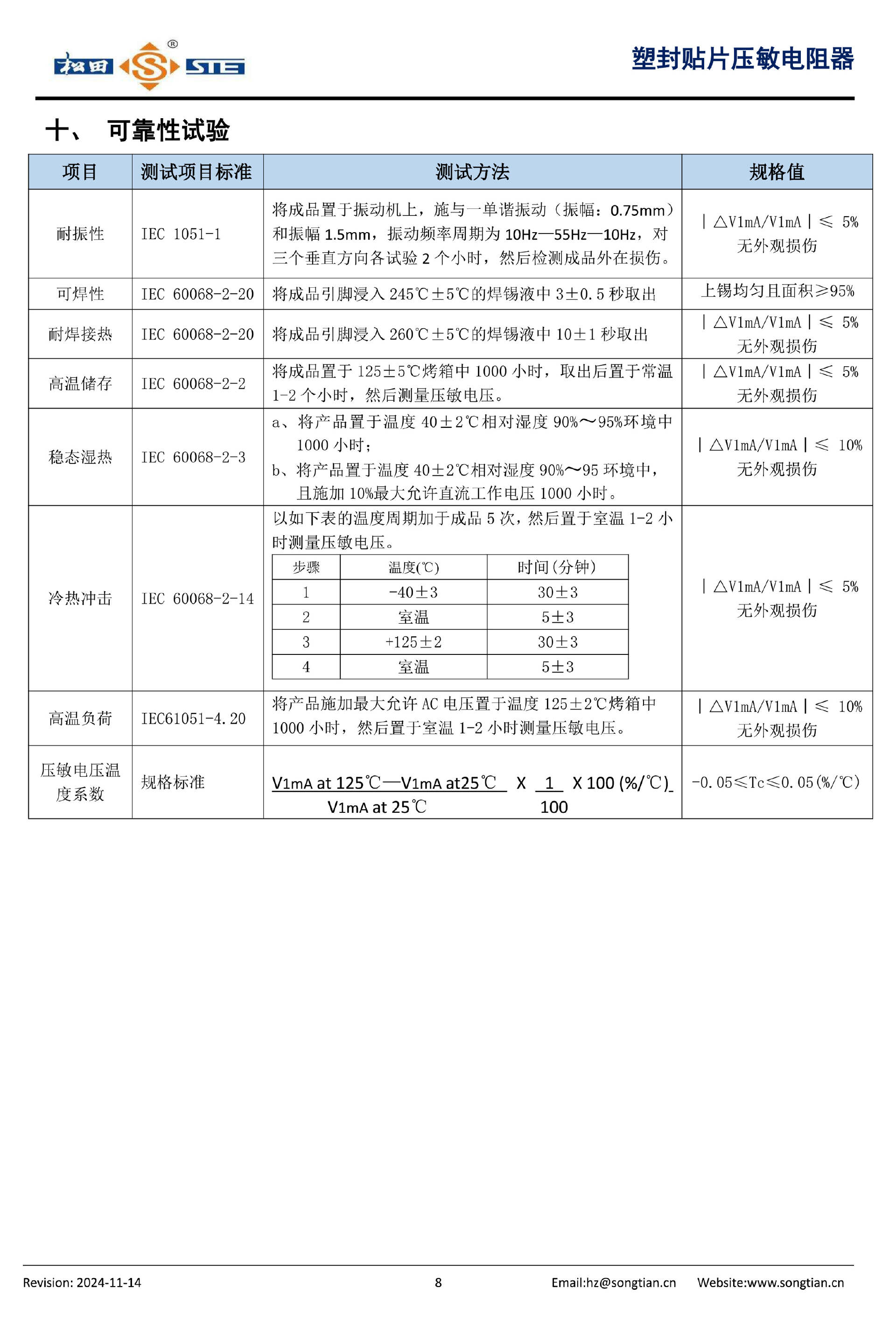
| Test | Source standard reference | Method | Acceptance criterion |
|---|---|---|---|
| Vibration | IEC 1051-1 | Sinusoidal vibration: the source states an amplitude of 0.75 mm and an amplitude of 1.5 mm; frequency sweep 10–55–10 Hz; 2 h in each of three perpendicular directions. Inspect for external damage. | |ΔV1mA/V1mA| ≤5%; no visible damage |
| Solderability | IEC 60068-2-20 | Immerse terminals in solder at 245±5°C for 3±0.5 s. | Uniform wetting over ≥95% of the area |
| Resistance to soldering heat | IEC 60068-2-20 | Immerse terminals in solder at 260±5°C for 10±1 s. | |ΔV1mA/V1mA| ≤5%; no visible damage |
| High-temperature storage | IEC 60068-2-2 | 1000 h at 125±5°C; recover at room temperature for 1–2 h, then measure varistor voltage. | |ΔV1mA/V1mA| ≤5%; no visible damage |
| Damp heat, steady state | IEC 60068-2-3 | a: 1000 h at 40±2°C, 90–95% RH. b: the same temperature and humidity, with 10% of the maximum permissible DC operating voltage for 1000 h. | |ΔV1mA/V1mA| ≤10%; no visible damage |
| Thermal shock | IEC 60068-2-14 | Apply the temperature cycle in the following table 5 times, then recover at room temperature for 1–2 h and measure varistor voltage. | |ΔV1mA/V1mA| ≤5%; no visible damage |
| High-temperature load | IEC6051-4.20 | Apply the maximum permissible AC voltage at 125±2°C for 1000 h; recover at room temperature for 1–2 h and measure varistor voltage. | |ΔV1mA/V1mA| ≤10%; no visible damage |
| Varistor-voltage temperature coefficient | Specification standard | [(V1mA at 125°C − V1mA at 25°C) / V1mA at 25°C] × (1/100) × 100 (%/°C) | -0.05≤Tc≤0.05 (%/°C) |
Standard references and the two vibration-amplitude statements are retained as printed; they are not verification of current standards or certification. The English humidity wording supplies the percent meaning missing from clause b in the image.
| Step | Temperature (°C) | Duration (min) |
|---|---|---|
| 1 | -40±3 | 30±3 |
| 2 | Room temperature | 5±3 |
| 3 | +125±2 | 30±3 |
| 4 | Room temperature | 5±3 |
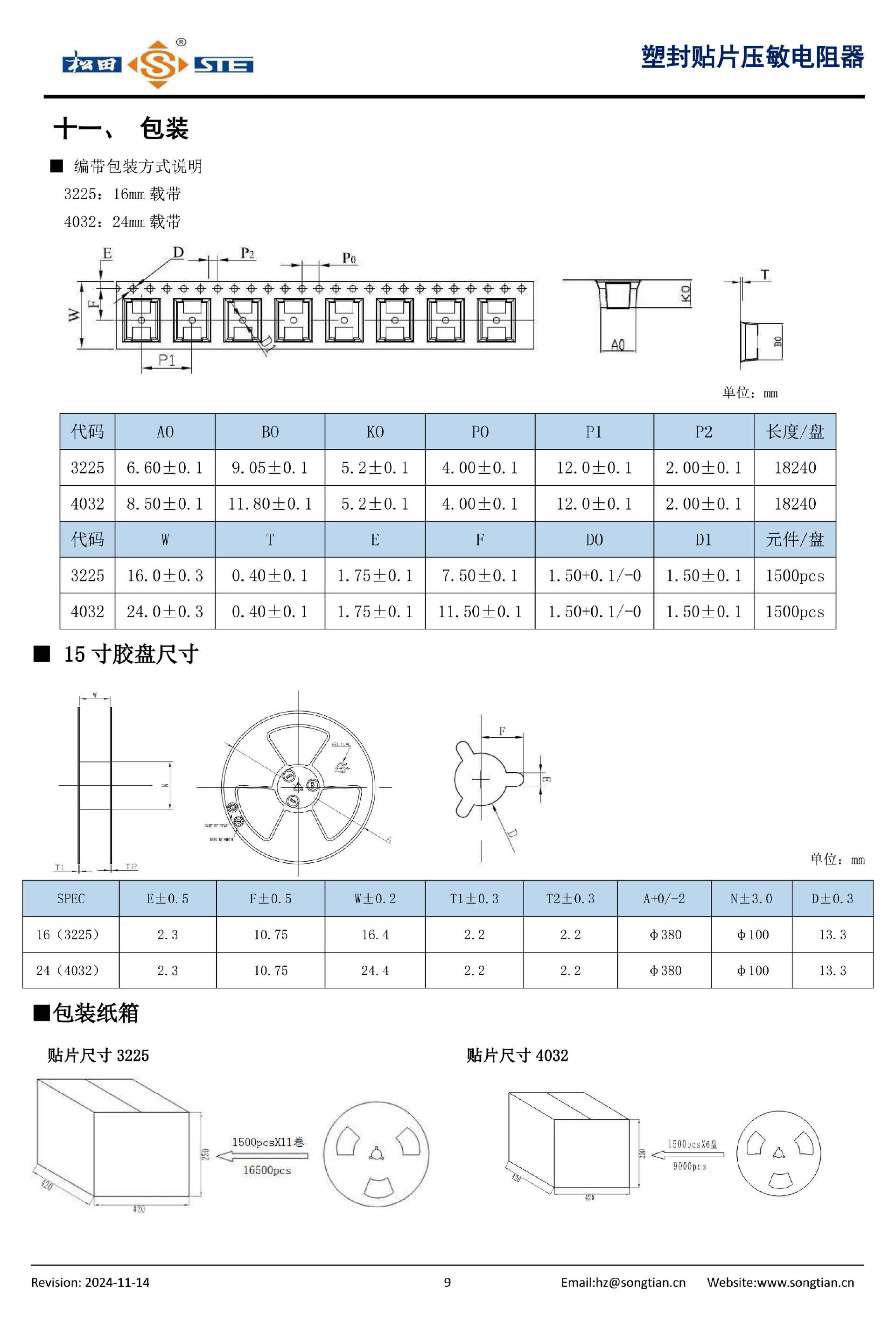
| Type | A0 | B0 | K0 | P0 | P1 | P2 | Length per reel |
|---|---|---|---|---|---|---|---|
| 3225 | 6.60±0.1 | 9.05±0.1 | 5.2±0.1 | 4.00±0.1 | 12.0±0.1 | 2.00±0.1 | 18240 |
| 4032 | 8.50±0.1 | 11.80±0.1 | 5.2±0.1 | 4.00±0.1 | 12.0±0.1 | 2.00±0.1 | 18240 |
| Type | W (mm) | T (mm) | E (mm) | F (mm) | D0 (mm) | D1 (mm) | Components per reel |
|---|---|---|---|---|---|---|---|
| 3225 | 16.0±0.3 | 0.40±0.1 | 1.75±0.1 | 7.50±0.1 | 1.50+0.1/-0 | 1.50±0.1 | 1500 pcs |
| 4032 | 24.0±0.3 | 0.40±0.1 | 1.75±0.1 | 11.50±0.1 | 1.50+0.1/-0 | 1.50±0.1 | 1500 pcs |
| Type | E±0.5 | F±0.5 | W±0.2 | T1±0.3 | T2±0.3 | A+0/-2 | N±3.0 | D±0.3 |
|---|---|---|---|---|---|---|---|---|
| 16 (3225) | 2.3 | 10.75 | 16.4 | 2.2 | 2.2 | φ380 | φ100 | 13.3 |
| 24 (4032) | 2.3 | 10.75 | 24.4 | 2.2 | 2.2 | φ380 | φ100 | 13.3 |
| Package | Carton dimensions (mm) | Reels per carton | Components per reel | Components per carton |
|---|---|---|---|---|
| 3225 | 420×420×250 | 11 | 1500 | 16500 |
| 4032 | 420×420×200 | 6 | 1500 | 9000 |
Related reading cited by the original report
Chinese source titles are retained below. 正浩、隆鑫两家知名户外电源品牌齐选松田元件 松田电子推出贴片式NTC热敏电阻器,可用于消费电子、工业设备等领域实现产品小型化 百款设备的共同选择,一文看懂松田元件历年拆解案例