
Design from R/T limits, not nominal B alone
The compensation residual depends on the full curve and its tolerances over the target interval. Obtain min./typ./max. R/T data or coefficients and model the actual network, reference and ADC errors.
| R25 | 5 Ω–500 kΩ |
|---|---|
| B25/50 | 2,600–4,750 K |
| B-value tolerance | ±10% |
| R25 tolerance | ±5% to ±20% |
| Operating temperature | −30 °C to +125 °C |
| Body size | 6.5 × 4.0 mm max. |
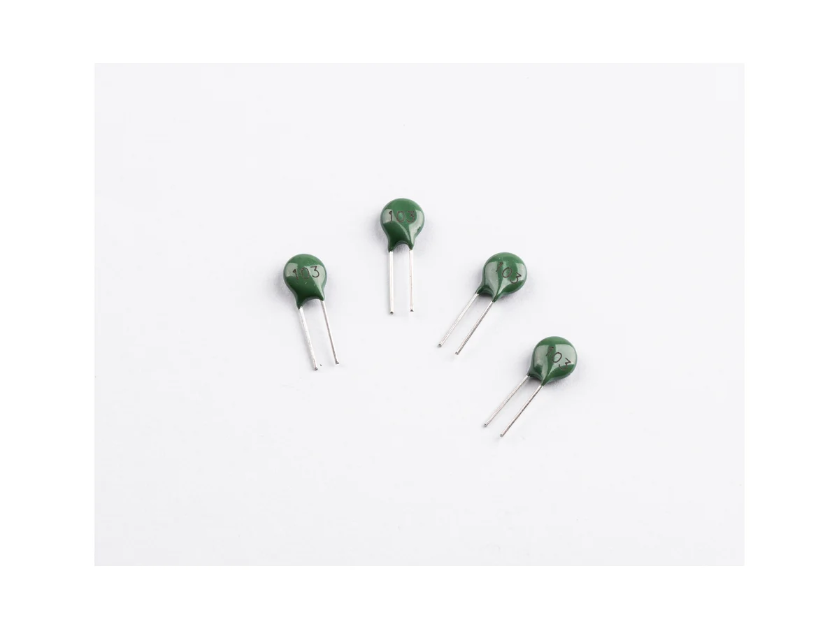
Radial dipped NTC thermistors for circuit temperature compensation and general temperature measurement. R25 5 Ω–500 kΩ, B25/50 2,600–4,750 K, operating temperature −30 °C to +125 °C.
Part-number list on request. Download the datasheet or send us your specification.
Send your specificationDatasheets, technical documents and approval certificates for this series. English editions of documents marked “Chinese” are available on request.
Radial dipped NTC thermistors for general temperature measurement and circuit temperature compensation. 14 B25/50 curves from 2,600 K to 4,750 K cover R25 5 Ω–500 kΩ; B-value tolerance ±10%. Body max. 6.5 mm wide and 4.0 mm thick. Operating temperature −30 °C to +125 °C.
| Function | Radial NTC thermistor for general temperature measurement and circuit temperature compensation |
|---|---|
| Environmental compliance | RoHS and REACH compliant; halogen status and material declarations on request |
| Packing | Bulk or taped |
| B25/50 curves | 14 curves, each covering one R25 range |
| B25/50 range | 2,600–4,750 K |
| B-value tolerance | ±10% |
| R25 range | 5 Ω–500 kΩ |
| Curve B25/50 2,600 K | R25 5–7 Ω |
| Curve B25/50 2,800 K | R25 8–24 Ω |
| Curve B25/50 3,000 K | R25 25–119 Ω |
| Curve B25/50 3,200 K | R25 120–359 Ω |
| Curve B25/50 3,600 K | R25 360–1,400 Ω |
| Curve B25/50 3,950 K | R25 1,500–5,900 Ω |
| Curve B25/50 4,050 K | R25 6,000–12,000 Ω |
| Curve B25/50 4,150 K | R25 13,000–17,000 Ω |
| Curve B25/50 4,300 K | R25 45,000–79,000 Ω |
| Curve B25/50 4,400 K | R25 80,000–144,000 Ω |
| Curve B25/50 4,500 K | R25 145,000–199,000 Ω |
| Curve B25/50 4,600 K | R25 200,000–299,000 Ω |
| Curve B25/50 4,750 K | R25 300,000–500,000 Ω |
| R25 tolerance | ±5% · ±10% · ±15% · ±20%; tolerances available per curve on request |
| Available values | R25 ranges are curve bands, not individual part numbers. |
| Temperature accuracy | R25 and B tolerances do not state a ±°C accuracy. Calculate the temperature error from the R/T table of the selected part number. |
| Zero-power resistance | DC resistance at temperature t, measured at a power low enough that any further reduction changes the resistance by less than 0.1% |
| Operating temperature | −30 °C to +125 °C |
| Thermal time constant | Approx. 30 s |
| Dissipation constant | Approx. 4.5 mW/°C |
| Body width | 6.5 mm max. |
| Body thickness | 4.0 mm max. |
| Lead spacing | 2.5 ±1.0 mm |
| Lead diameter | 0.45 mm (nom.) |
| Lead length | ≥25 mm from the body |
| Coating | Dipped coating |
| Coating insulation | No insulation rating is specified for the coating. Qualify it before relying on it for isolation. |
| Wave soldering, preheat | Ambient to 130 ±20 °C in 30–90 s; 1–3 °C/s |
| Wave soldering, ramp to peak | 130 ±20 °C to 260 °C max. in <1 s (approx. 200 °C/s) |
| Wave soldering, dwell | <10 s at peak |
| Wave soldering, cooling | 5 °C/s max. |
| Hand soldering and rework | Iron tip 300 °C max. · 3 s max. · joint at least 2 mm from the coating |
| Handling | Do not touch the thermistor while it is energized. |
| Storage | ≤35 °C · ≤70% RH · 12 months · keep the original package closed and reseal after opening |
| Corrosive atmospheres | Hydrogen chloride, hydrogen sulfide and sulfur compounds can degrade terminal solderability. Avoid exposure. |
| Further data | On request: nominal R25, B value, tolerance and resistance–temperature (R/T) table of each part number · measuring medium and conditions for the thermal time constant and dissipation constant · max. power at 25 °C, power derating, max. measuring current and voltage, allowed self-heating · max. working voltage, insulation resistance and dielectric withstand · coating material, flammability and insulation properties · lead alloy, plating and solderability class · recommended PCB hole pattern · packing method, quantity and taping dimensions · wave-soldering solder alloy, immersion depth and number of cycles · post-solder resistance limits, cleaning compatibility, lead forming and conformal-coating or potting compatibility · load-life, high- and low-temperature storage, thermal-shock, damp-heat, vibration, lead-strength, solderability and long-term drift results · temperature coefficient α, linearization range and example compensation networks |
Ranges by dielectric, package and lead style within this series.
| Variant | Body dimensions | R25 range | Tolerance | Lead / land pattern | Notes |
|---|---|---|---|---|---|
| B25/50 2600 K | 6.5 max. × 4.0 max. mm, radial | R25 5–7 Ω | B ±10%; R25 tolerance per part number | Leads Ø0.45 mm · spacing 2.5 ±1 mm · ≥25 mm long | Very low resistance, for low-ohm compensation. |
| B25/50 2800 K | Same outline | R25 8–24 Ω | B ±10%; R25 tolerance per part number | Same leads | Low resistance, low B value. |
| B25/50 3000 K | Same outline | R25 25–119 Ω | B ±10%; R25 tolerance per part number | Same leads | Low-resistance compensation. |
| B25/50 3200 K | Same outline | R25 120–359 Ω | B ±10%; R25 tolerance per part number | Same leads | Sub-kilohm compensation. |
| B25/50 3600 K | Same outline | R25 360–1,400 Ω | B ±10%; R25 tolerance per part number | Same leads | Low-kilohm compensation. |
| B25/50 3950 K | Same outline | R25 1.5–5.9 kΩ | B ±10%; R25 tolerance per part number | Same leads | Mid B value. Select the nominal R25 and R/T data. |
| B25/50 4050 K | Same outline | R25 6–12 kΩ | B ±10%; R25 tolerance per part number | Same leads | Nominal 10 kΩ region. |
| B25/50 4150 K | Same outline | R25 13–17 kΩ | B ±10%; R25 tolerance per part number | Same leads | Higher sensitivity. |
| B25/50 4300 K | Same outline | R25 45–79 kΩ | B ±10%; R25 tolerance per part number | Same leads | High-resistance compensation. |
| B25/50 4400 K | Same outline | R25 80–144 kΩ | B ±10%; R25 tolerance per part number | Same leads | High-resistance compensation. |
| B25/50 4500 K | Same outline | R25 145–199 kΩ | B ±10%; R25 tolerance per part number | Same leads | High B value. |
| B25/50 4600 K | Same outline | R25 200–299 kΩ | B ±10%; R25 tolerance per part number | Same leads | High resistance, high B value. |
| B25/50 4750 K | Same outline | R25 300–500 kΩ | B ±10%; R25 tolerance per part number | Same leads | Highest R25 and B value. Check leakage and noise in the circuit. |
Start with the compensation interval, the permitted residual error of the circuit and the thermal location. Then select nominal R25, B25/50 and tolerance, and design with the R/T data, excitation limits and construction details of the selected part.
Specify temperature interval, nominal compensation point, required residual error, source impedance, ADC and reference or analog network, response, self-heating, life, humidity and the thermal and mechanical PCB environment.
Choose nominal R25 and B25/50 from the 14 curves. Evaluate the R/T table (min./typ./max.), temperature coefficient, temperature error, interpolation and drift of the selected part number.
Use the full curve to limit current, voltage, power and self-heating at every temperature. Correlate the approx. 30 s and 4.5 mW/°C values with the actual PCB location, airflow and lead heat path.
Define coating and insulation, lead alloy and plating, body and lead tolerances, hole pattern, packing, forming limits and the wave- or hand-soldering, cleaning and coating process.
Validate curve accuracy, compensation residual, power derating, humidity with bias, dry heat, thermal cycling and shock, vibration, lead strength, solderability, process shift and long-term drift.
The compensation residual depends on the full curve and its tolerances over the target interval. Obtain min./typ./max. R/T data or coefficients and model the actual network, reference and ADC errors.
Obtain the rated power and measuring current of the selected part. Calculate the excitation at worst-case resistance and temperature, use duty cycling where possible and verify the body temperature rise on the board.
The dipped coating has no specified insulation, flammability or potting-compatibility rating. Obtain coating and lead materials and qualify humidity, cleaning, conformal coating and electrical isolation.
Validate solder alloy, flux, board, immersion depth, preheat, 260 °C peak, <10 s dwell, cooling, lead forming and post-solder R/T shift for the packed part.
Define carrier pitch, orientation and quantity or bulk insertion controls, hole pattern, seating plane, lead form and marking before production.