S

S Series Standard Radial-Leaded Metal-Oxide Varistors

Nominal varistor voltage18–1,100 V
Max. peak current (8/20 µs)100–6,500 A
Max. continuous voltage11–680 VAC / 14–895 VDC
Max. energy (10/1000 µs)0.4–383 J
Disc size05D–20D
Operating temperature−40 °C to +105 °C
UL certification markCQC certification mark

Radial-leaded zinc-oxide disc varistors, 05D–20D, for board-level transient suppression; varistor voltage 18–1,100 V, max. peak current 6,500 A (8/20 µs).

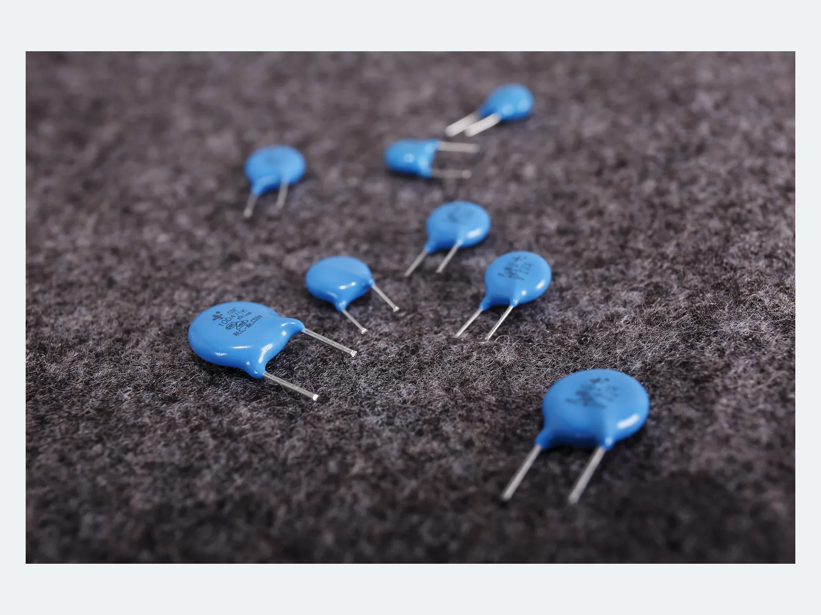
Series product photograph

Part numbers

1,409

Showing 24 of 1,409 part numbers

STE05D180K1BN0FSB0R051811144011000.40.015
STE05D180K1BQ0FST0R051811144011000.40.015
STE05D180K1BQ0FSTRR051811144011000.40.015
STE05D220K1BN0FSB0R052214184811000.50.015
STE05D220K1BQ0FST0R052214184811000.50.015
STE05D270K1BN0FSB0R052717226011000.60.015
STE05D270K1BN0FSBTR052717226011000.60.015
STE05D270K1BQ0FST0R052717226011000.60.015
STE05D330K1BN0FSB0R053320267311000.80.015
STE05D330K1BQ0FST0R053320267311000.80.015
STE05D390K1BN0FSB0R053925318011000.90.015
STE05D390K1BQ0FST0R053925318011000.90.015
STE05D390K1BQ0FSTKR053925318011000.90.015
STE05D470K1BN0FSB0R0547303810411001.10.015
STE05D470K1BN0FSBTR0547303810411001.10.015
STE05D470K1BQ0FST0R0547303810411001.10.015
STE05D560K1BN0FSB0R0556354512311001.30.015
STE05D560K1BQ0FST0R0556354512311001.30.015
STE05D680K1BN0FSB0R0568405614511001.60.015
STE05D820K1BN0FSB0R0582506515054002.50.15
STE05D820K1BN0FSBTR0582506515054002.50.15
STE05D820K1BQ0FST0R0582506515054002.50.15
STE05D820K3BA5FSB0R0582506515054002.50.15
STE05D101K1BN0FSB0R051006085175540030.15

— = not specified

Need a value that is not listed? Send us your specification.

Datasheets & approval documents

Datasheets, technical documents and approval certificates for this series. English editions of documents marked “Chinese” are available on request.

Need a document not listed here? Ask us

Engineering details

Overview

Radial-leaded metal-oxide varistors with epoxy-coated zinc-oxide discs for board-level transient voltage suppression. Disc sizes 05D to 20D, nominal varistor voltage 18–1,100 V, max. continuous voltage 11–680 VAC / 14–895 VDC. Max. peak current 100–6,500 A (8/20 µs, one pulse), max. energy 0.4–383 J (10/1000 µs). Operating temperature −40 °C to +105 °C.

Series features

  • Five disc sizes: 05D, 07D, 10D, 14D and 20D
  • Max. continuous AC/DC voltage, varistor voltage, clamping voltage, 8/20 µs peak current and 10/1000 µs energy specified per part number
  • Operating temperature −40 °C to +105 °C; 12-month storage life
  • CQC and VDE certified, UL/cUL recognized to UL 1449; coverage depends on the part number
Specifications
FunctionRadial-leaded zinc-oxide varistor for transient voltage clamping; voltage-dependent shunt element with finite pulse life
ConstructionEpoxy-coated zinc-oxide disc with radial leads
Reference standardsGB/T 10193 · GB/T 10194 · GB 8898-2011 · GB 4943.1-2011 · UL 1449 · IEC 61051 · IEC 60950-1:2013
Disc sizes05D · 07D · 10D · 14D · 20D
Nominal varistor voltage18–680 V (05D) · 18–820 V (07D) · 18–1,100 V (10D, 14D, 20D)
Max. continuous voltage11–680 VAC · 14–895 VDC; per disc size and voltage code
Varistor voltage measured at0.1 mA (05D) · 1 mA (07D, 10D, 14D, 20D)
Varistor-voltage toleranceK = ±10%. Some low-voltage types have asymmetric limits (see datasheet).
Max. clamping voltageSpecified per part number at test current IP. Compare clamping voltages only at the same current and waveform.
Max. peak current, 8/20 µs, one pulse100–6,500 A; per disc size and voltage code
Max. peak current, 8/20 µs, two pulses50–4,500 A. Not a repetitive-pulse rating.
Max. energy absorption, 10/1000 µs0.4–383 J; per part number
Rated power0.01–1.0 W, depending on disc size and voltage
Capacitance (typical)38–28,500 pF at 1 kHz
Waveform ratings8/20 µs current and 10/1000 µs energy ratings are separate tests. Do not convert either to another waveform or to repetitive duty.
Operating temperature−40 °C to +105 °C
Storage≤35 °C · ≤70% RH · no corrosive gas or direct sunlight · 12 months max.
Dimensions, 05DD max. 7.5 mm · T max. 3.5–5.5 mm · lead pitch F 5.0 ±0.5 mm · lead Ø d 0.5 ±0.05 mm
Dimensions, 07DD max. 9.0 mm · T max. 3.5–5.5 mm · lead pitch F 5.0 ±0.5 mm · lead Ø d 0.5 ±0.05 mm
Dimensions, 10DD max. 12.5 mm · T max. 4.0–7.5 mm · lead pitch F 7.5 ±0.5 mm · lead Ø d 0.7 ±0.05 mm
Dimensions, 14DD max. 16.0 mm · T max. 4.0–7.5 mm · lead pitch F 7.5 ±0.5 mm · lead Ø d 0.7 ±0.05 mm
Dimensions, 20DD max. 23 mm (18–68 V), 21 mm (from 82 V) · T 4.0–8.0 mm · lead pitch F 10 ±0.5 mm · lead Ø d 1.0 mm straight / 0.8 mm bent, ±0.05 mm
Lead formsLong straight · single outward bend · short straight · front/rear raised
Lead lengthLong straight ≥16 mm; short or bent 2.5–<6 mm ±0.5 mm or 6–10 mm ±1.0 mm. Coating run-down and bend height depend on the lead form.
PackingBulk or taped; taping for 5, 7.5 and 10 mm lead pitch
TapingComponent pitch 12.7 or 25.4 mm, depending on lead pitch · carrier width 18 mm · H0 16.5 / 17 / 19 / 20 mm
Hand soldering and rework350 °C max. · 3 s max. · solder point at least 2 mm from the coating
Flame classClass C per CQC approval, for covered constructions
End-of-life protectionLeakage current and clamping voltage can change after surges. Coordinate upstream overcurrent protection or a thermal disconnector.
Further dataOn request: rated-power derating versus ambient temperature · peak-current and energy derating versus pulse count, pulse width and interval · wave-soldering, preheat, cleaning and conformal-coating conditions · failure-mode data · endurance, damp-heat, thermal-cycling, vibration, lead-strength and solderability results
Variants

Ranges by dielectric, package and lead style within this series.

VariantBody dimensionsVaristor voltage / max. continuous voltagePeak current (8/20 µs, one pulse) / energy (10/1000 µs) / rated powerLead / land patternNotes
05DD max. 7.5 mm · T max. 3.5–5.5 mm18–680 V · 11–420 VAC · 14–560 VDC100–400 A · 0.4–19 J · 0.01–0.1 WF 5.0 ±0.5 mm · d 0.5 ±0.05 mmSmallest disc, for lower surge energy. Clamping voltage and capacitance per part number.
07DD max. 9.0 mm · T max. 3.5–5.5 mm18–820 V · 11–510 VAC · 14–670 VDC250–1,200 A · 0.9–42 J · 0.02–0.25 WF 5.0 ±0.5 mm · d 0.5 ±0.05 mmCompact general-purpose size.
10DD max. 12.5 mm · T max. 4.0–7.5 mm18–1,100 V · 11–680 VAC · 14–895 VDC500–2,500 A · 2.1–115 J · 0.05–0.4 WF 7.5 ±0.5 mm · d 0.7 ±0.05 mmMid-size disc balancing board area, surge current and energy.
14DD max. 16.0 mm · T max. 4.0–7.5 mm18–1,100 V · 11–680 VAC · 14–895 VDC1,000–4,500 A · 4–213 J · 0.1–0.6 WF 7.5 ±0.5 mm · d 0.7 ±0.05 mmHigher surge current for industrial and appliance inputs. Coordinate pulse life and fail-safe protection.
20DD max. 23 mm (18–68 V), 21 mm (from 82 V) · T max. 4.0–8.0 mm18–1,100 V · 11–680 VAC · 14–895 VDC2,000–6,500 A · 11–383 J · 0.2–1.0 WF 10 ±0.5 mm · d 1.0 mm straight / 0.8 mm bent, ±0.05 mmHighest energy in the series. Coordinate fusing or thermal protection and the soldering process.
Selection guide

Select the max. continuous AC/DC voltage first. Then match varistor voltage, clamping voltage at the actual surge current, pulse shape, energy, repetition, temperature and end-of-life protection. The disc size follows from the surge stress and the required pulse life.

  1. Define continuous and temporary overvoltage

    State nominal and max. AC/DC voltage, frequency, tolerance, grounding, harmonics, temporary-overvoltage duration and abnormal conditions. Select from the max. continuous voltage, not from the nominal varistor voltage.

  2. Define the surge waveform and surge source

    State open-circuit voltage, short-circuit current, source impedance, current waveform (8/20 µs or other), voltage waveform (1.2/50 µs or other), polarity, repetition, interval and expected number of events.

  3. Coordinate clamping with the protected load

    Use the clamping voltage at its stated test current and include lead and PCB inductance. Check semiconductor absolute maximum ratings, insulation, downstream capacitors and creepage at the actual surge current.

  4. Check energy, temperature and pulse life

    An energy rating at 10/1000 µs does not define life under repetitive 8/20 µs or other pulses. Include derating versus pulse count and temperature, leakage drift and end-of-life criteria in the mission profile.

  5. Specify mechanics and fail-safe protection

    Specify disc size, voltage code, lead form and length, packing, drawing and approval for each part number. Coordinate fusing or thermal disconnection, flame containment, spacing, soldering process and service replacement.

Approvals & reliability

Approvals & qualifications

Approval coverage depends on disc size, voltage range and lead construction.

AgencyStandardCertificateScope
CQC certification markCQCGB/T 10193 · GB/T 10194 · GB 8898 · GB 4943.105D 19001213185 · 07D 19001213190 · 10D 19001213188 · 14D 19001213191 · 20D 19001213192Nominal varistor voltage 82–560 V (05D), 82–820 V (07D) and 82–1,100 V (10D, 14D, 20D), with construction-specific conditions. 10D/14D/20D certificates valid to 31 Oct 2027, subject to surveillance.
UL certification markUL / cULUL 1449E330837Recognized component. Coverage varies by model, voltage code, lead style and coating.
VDE certification markVDEIEC 61051 · IEC 60950-1:201340023049Covers defined disc sizes and voltage values, not the complete series.

Each certificate covers the types and ratings listed on it.

Design notes

Select from continuous voltage, not V1mA

Nominal varistor voltage is a measurement point, not a permissible operating voltage. Include line tolerance, frequency, harmonics, grounding and temporary overvoltage when selecting the max. continuous VAC/VDC.

Use clamping voltage at the actual current

Residual voltage depends on surge current, dynamic resistance and interconnect inductance. Use the clamping voltage at its stated test current, then verify at the protected node on the production PCB with the actual source impedance.

Do not mix waveform ratings

Peak current is rated at 8/20 µs and energy at 10/1000 µs. Do not convert either to another pulse shape without a derating model from STE. Repetition and previous stress reduce capability.

Design for degradation and safe end of life

Leakage current and clamping voltage can change after surges. Coordinate upstream overcurrent protection or a thermal disconnector, fire containment, abnormal overvoltage and an inspection or replacement policy.

Coordinate the complete surge-protection stage

Define the equipment surge standard, source impedance, common and differential mode, insulation, spacing, grounding and downstream withstand. A board-level varistor alone does not establish an IEC/UL SPD class or equipment-level compliance.

Control lead geometry and soldering heat

Keep leads short to limit inductive overshoot without stressing the coating. Specify lead form, lead length and tape geometry with the part number. Validate wave or hand soldering, cleaning and coating. Observe the 12-month storage limit.

Part numbering

Example ordering code. Not every combination is available.

STE · 10 · D · 471 · K · 1 · E · N0 · F · S · B · 0 · R · 0

CodeMeaning
STESTE prefix
10Disc diameter: 10 = 10 mm; 05, 07, 14, 20 for the other sizes
DDisc shape
471Nominal varistor voltage: 471 = 470 V; 220 = 22 V, 112 = 1,100 V
KVaristor-voltage tolerance: K = ±10%
1Lead form: 1 = long straight; 2 = single outward bend, 3 = short straight, 8 = front/rear raised
ELead pitch: E = 7.5 mm; B = 5.0 mm, D = 10.0 mm
N0Lead length or taped height; the code depends on bulk or taped packing (code list on request)
FLead material: F = tin-plated copper-clad steel; C = copper wire
SVaristor type: S = standard series
BPacking: B = bulk; T = taped
0Factory code, assigned by STE
REnvironmental code: R = RoHS; F = RoHS and halogen-free
0Factory code, assigned by STE