
Check that PET suits the duty
PET offers compact high capacitance, but its loss, dielectric absorption and temperature and frequency behavior differ from polypropylene. Validate the actual signal, ripple and drift requirements.
| Rated voltage | 100 / 250 / 400 / 630 VDC |
|---|---|
| Capacitance | 10 nF–10 µF |
| Operating temperature | −40 °C to +125 °C |
| Dielectric | Metallized PET |
| Tolerance | ±5% / ±10% |
| Lead spacing | 7.5–27.5 mm |
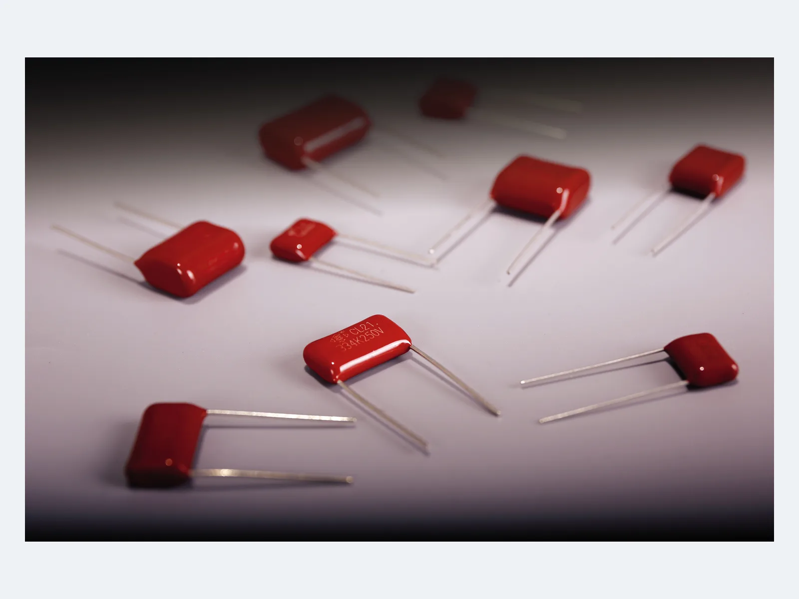
General-purpose epoxy-dipped metallized polyester (PET) film capacitors for bypass, blocking, coupling and filtering. 100–630 VDC, 10 nF–10 µF.
Showing 25 of 788 part numbers
| L21H474JQ135170140070EOZ |
|---|
| L21J105JJ1B0095085050EOY |
| L21J105JJ1B0095085050EOZ |
| L21J105JJ1B0095095065EOY |
| L21J334JJ1B0095085050EOJ |
| L21J335KN1B0120125080EOJ |
| L21J335KQ1B0170160080EOJ |
| L21T104KN1B0120095050EOJ |
| L21T104KN235120095050EOJ |
| L21T105JQ135170170100EOJ |
| L21T154JN135120105060EOJ |
| L21T154KN235120105060EOJ |
| L21T155KQ138170195095EOJ |
| L21T224JN1B0120115065EOJ |
| L21T224JN235120095050EOA |
| L21T224KN135120120070EOJ |
| L21T224KN235120120070EOJ |
| L21T334JN135120140070EOJ |
| L21T334JN1B0120140070EOJ |
| L21T474JN335170155090EOJ |
| L21T474KQ135170105055EOZ |
| L21T474KQ135170135070EOJ |
| L21T684JN138120175085EOJ |
| L22A104JJ1B0095075045EOY |
| L22A104JN1B0120085045EAJ |
Need a value that is not listed? Send us your specification.
Datasheets, technical documents and approval certificates for this series. English editions of documents marked “Chinese” are available on request.
Metallized polyester (PET) film capacitors with a non-inductive, self-healing winding and epoxy-resin dip coating, for bypass, blocking, coupling, filtering and low-pulse circuits. Rated 100, 250, 400 and 630 VDC, 10 nF–10 µF, J ±5% or K ±10%. Lead spacing 7.5–27.5 mm. Operating temperature −40 °C to +125 °C, with voltage derating above +105 °C.
| Product type | General-purpose metallized polyester DC film capacitor for bypass, blocking, coupling, filtering and low-pulse circuits; not a safety capacitor, not for reflow soldering |
|---|---|
| Construction | Metallized polyethylene terephthalate (PET) film · non-inductive winding · epoxy-resin dipped radial body |
| Self-healing | Yes |
| Rated DC voltage | 100 · 250 · 400 · 630 VDC |
| Capacitance range | 100 VDC: 10 nF–10 µF · 250 VDC: 10 nF–4.7 µF · 400 VDC: 10 nF–3.3 µF · 630 VDC: 10 nF–1.5 µF |
| Capacitance tolerance | J ±5% · K ±10% |
| Operating temperature | −40 °C to +125 °C |
| Voltage derating above +105 °C | 1.25% of UR per °C from +105 °C to +125 °C; 75% of UR at +125 °C when applied linearly. Derating curve on request. |
| Climatic category | 40/100/21 |
| Storage temperature | +15 °C to +35 °C |
| Dissipation factor | tan δ ≤1.0% at 1 kHz, 1.0 Vrms, 20 °C |
| Insulation resistance, UR >100 V, C ≤0.33 µF | ≥30,000 MΩ at 100 VDC, 60 s, 20 °C |
| Insulation resistance, UR >100 V, C >0.33 µF | Time constant IR × C ≥10,000 s at 100 VDC, 60 s, 20 °C |
| Insulation resistance, UR ≤100 V, C ≤0.33 µF | ≥15,000 MΩ at 100 VDC, 60 s, 20 °C |
| Insulation resistance, UR ≤100 V, C >0.33 µF | Time constant IR × C ≥5,000 s at 100 VDC, 60 s, 20 °C |
| Voltage proof, terminal to terminal | 1.6 × UR for 5 s |
| Pulse ratings | Designed for low-pulse duty |
| AC operation | DC-rated only; do not use in AC, resonant or capacitive-dropper circuits without frequency, current and lifetime data from STE |
| Safety class | No X/Y class and no agency approval; do not use across the line or line to earth |
| Coating | Epoxy resin |
| Body dimensions | W 10–31 · H 8–23 · T 4.5–13.5 mm, depending on voltage and capacitance |
| Lead spacing | 7.5 · 10 · 15 · 20 · 22.5 · 27.5 mm, ±1.0 mm |
| Lead diameter | 0.6 ±0.05 mm at 7.5 / 10 mm spacing · 0.8 ±0.05 mm at 15–27.5 mm spacing |
| Lead forms and packing | Long straight · inner-bent · straight taped · bent taped |
| Taping | Tape dimensions specified for 7.5, 10, 15 and 20–22.5 mm lead spacing; 27.5 mm packing on request |
| Soldering profile, PP | Preheat ≤110 °C · soldering ≤120 °C · ≤15 s |
| Soldering profile, PE | Preheat ≤125 °C · soldering ≤160 °C · ≤15 s |
| Hand soldering | 350 °C max. · 3 s max. · ≥2 mm from the coating |
| Reflow soldering | Not permitted; film shrinkage can degrade performance |
| Environmental compliance | RoHS and REACH compliant; bromine-free and halogen-free. Material declarations on request. |
| Further data | On request: clearing energy, capacitance loss and end-of-life limits · storage humidity and shelf life · dV/dt, K0, peak and repetitive current, pulse energy and repetition rate · ESR, ESL, impedance, self-resonant frequency, permissible voltage and current versus frequency, thermal resistance and temperature rise · capacitance and dissipation factor versus temperature and frequency, dielectric absorption, drift and DC-bias curves · UL 94 class · loaded-life, high-temperature endurance, pulse-life, damp-heat, overload, thermal-cycle, vibration and lead-strength test results |
Ranges by dielectric, package and lead style within this series.
| Variant | Body dimensions | Rated voltage / capacitance | Dielectric / tolerance | Lead / land pattern | Notes |
|---|---|---|---|---|---|
| J · 7.5 mm | W 10 · H 8–10.5 · T 4.5–6.5 mm | 100 VDC: 10–100 nF · 250 VDC: 10–68 nF · 400 VDC: 10–15 nF | Metallized PET · J/K | P 7.5 ±1.0 · d 0.6 ±0.05 mm | Smallest body; 5 mm lead spacing on request. |
| N · 10 mm | W 13 · H 9–13 · T 5–7.5 mm | 100 VDC: 150–680 nF · 250 VDC: 100–220 nF · 400 VDC: 22–150 nF · 630 VDC: 10–68 nF | Metallized PET · J/K | P 10 ±1.0 · d 0.6 ±0.05 mm | Compact size; check frequency loss and temperature rise for the actual waveform. |
| Q · 15 mm | W 18 · H 11.5–16 · T 6–9 mm | 100 VDC: 1–2.2 µF · 250 VDC: 330 nF–1 µF · 400 VDC: 220–680 nF · 630 VDC: 100–330 nF | Metallized PET · J/K | P 15 ±1.0 · d 0.8 ±0.05 mm | Mid-range values for filtering and coupling; validate PET loss, drift and ripple current. |
| S · 20 mm | W 23 · H 15.5–20 · T 8.5–10.5 mm | 100 VDC: 3.3–4.7 µF · 250 VDC: 1.2–2.2 µF · 400 VDC: 1–1.2 µF · 630 VDC: 470–680 nF | Metallized PET · J/K | P 20 ±1.0 · d 0.8 ±0.05 mm | Higher capacitance; check temperature, ripple current and lead support. |
| T · 22.5 mm | W 25 · H 18–21 · T 11.5–12 mm | 100 VDC: 6.8 µF · 250 VDC: 3.3 µF · 400 VDC: 1.5 µF · 630 VDC: 1 µF | Metallized PET · J/K | P 22.5 ±1.0 · d 0.8 ±0.05 mm | Tape dimensions specified; verify case temperature and vibration support. |
| V · 27.5 mm | W 31 · H 19–23 · T 11.5–13.5 mm | 100 VDC: 10 µF · 250 VDC: 4.7 µF · 400 VDC: 2.2–3.3 µF · 630 VDC: 1.2–1.5 µF | Metallized PET · J/K | P 27.5 ±1.0 · d 0.8 ±0.05 mm | Largest body; packing on request. Support the body mechanically. |
Start with the duty (signal, filtering or low pulse) and whether PET suits it. Then check DC voltage, capacitance, frequency loss, pulse current, derating above +105 °C, dielectric drift, lifetime and dimensions.
Specify DC bias, AC ripple, frequency spectrum, peak voltage, rise and fall time, dV/dt, repetition rate, RMS current, abnormal transients, ambient and case temperature, cooling and required service hours.
The series covers 100–630 VDC, 10 nF–10 µF and 7.5–27.5 mm lead spacing. For other voltages, values below 10 nF, or 5 and 12.5 mm lead spacing, request the part specification.
Use Ipk = C·dV/dt and the measured spectrum. Obtain dV/dt, repetitive current, ESR, impedance, self-resonance, temperature rise, dielectric absorption and capacitance and loss drift for the selected part number.
Reduce the rated voltage by 1.25% per °C above +105 °C. Check the derating curve, maximum case or hot-spot temperature and loaded-life data against the actual waveform and target hours.
Match the part number to voltage, capacitance, tolerance, W/H/T, lead spacing, lead diameter and form, packing and soldering profile. Do not use reflow soldering; validate lead forming, cleaning, coating compatibility, vibration and thermal cycling.
PET offers compact high capacitance, but its loss, dielectric absorption and temperature and frequency behavior differ from polypropylene. Validate the actual signal, ripple and drift requirements.
Low pulse is not a defined limit. Calculate I = C·dV/dt and obtain dV/dt, repetitive-current, ESR and temperature-rise limits for the part number.
Select the limit by rated voltage and by capacitance above or below 0.33 µF. A single fixed resistance value does not apply across the whole capacitance range.
Applied linearly, the 1.25%/°C derating reaches 75% of rated voltage at +125 °C. Obtain the derating curve and loaded-life data; the temperature rating alone does not prove service life.
For voltages other than 100–630 VDC, values below 10 nF, or 5 and 12.5 mm lead spacing, request the construction, drawing, loss and current limits and qualification report.
Do not use reflow soldering. Apply the PP/PE soldering limits to the actual part, keep lead-forming stress away from the epoxy seal, and validate cleaning, coating, vibration and thermal cycling.
Example ordering code. Not every combination is available.
L2 · 2G · 104 · J · N · 1 · B0 · 130 · 105 · 055 · E · 0 · Z
| Code | Meaning |
|---|---|
| L2 | Series code: MEF/CL21 |
| 2G | Rated voltage code: 2G = 400 VDC; 2A = 100 VDC, 2E = 250 VDC, 2J = 630 VDC |
| 104 | Capacitance code: 104 = 100 nF; maximum value depends on voltage |
| J | Capacitance tolerance: J = ±5%, K = ±10% |
| N | Lead spacing: N = 10 mm; J = 7.5, Q = 15, S = 20, T = 22.5, V = 27.5 mm |
| 1 | Lead form: 1 = long straight, 2 = inner-bent, 5 = straight taped, 6 = bent taped |
| B0 | Lead length code: B0 = 20.0 mm |
| 130 | Body width: 130 = 13.0 mm |
| 105 | Body height: 105 = 10.5 mm |
| 055 | Body thickness: 055 = 5.5 mm |
| E | Environmental code: E = RoHS, F = RoHS and halogen-free |
| 0 | STE internal control code, first field |
| Z | STE internal control code, second field |